


Sponsored by Littelfuse
By Dr. Martin Schulz, Global Principal, Application Engineering, Littelfuse and Philippe Di Fulvio, Business Development Manager, Electric Vehicle Infrastructure, Littelfuse
For greater consumer acceptance of electric vehicles (EVs), designers need to solve the challenge of fast charging to minimize vehicle downtime, especially for long-distance driving. To achieve fast charging, designers need to increase charger power output, power density, and efficiency. Single-unit, charger designs range from 7 kW to 30 kW. Combining single-unit assemblies into modular designs increases power output and enables charger manufacturers’ goals for a smaller footprint, higher flexibility, and scalability. Using active power components in advanced, isolated packaging addresses the high-power charging challenges by enabling higher power density and significantly reducing the efforts in thermal management in circuit designs.
The increase in EV usage is also a challenge for electric utilities to manage the large loads resulting from re-charging EV batteries. Utilities are investigating two vehicle-to-grid technologies. The first technology, V1G, is known as smart charging. In this technology, the utilities will distribute the energy load to minimize demand peaks by controlling the time when charging an EV starts and the magnitude of the supplied energy. The second technology, V2G, bi-directional charging, would control the time and volume of charging and the direction of charging. The utility could pull power from a charged battery back to the grid to supply power to another vehicle to reduce peak demand. This approach could be cost-efficient for vehicle fleets as contributing to peak-shaving can be considered a valuable service. For example, most school buses run only during the day and are available for charging and sharing power all night. Larger fleet, like the 500,000 school buses operated in the US, could be controlled as highly decentralized energy storage. With 100 days idling during the US summer vacation, the battery capacity available can grow to a regime of GWh. In preparation for V2G technology, designers will need to develop bi-directional chargers that also can supply energy to the power grid. Compared to uni-direction chargers, bi-directional designs are more complex, requiring more components, additional effort to manage power dissipation, and sophisticated control algorithms.
Handling higher power requires advanced packaging of high-power semiconductors
Figure 1 illustrates a bi-directional power supply topology that employs 16 SiC power MOSFETs in sets of eight half-bridges. Designers can utilize more discrete power FETs in parallel to achieve higher power, making the charging/discharging system design much more difficult. The discrete power FET packaging is typically a D²PAK or a TO-247 package. When designing for output power level exceeding 30 kW, advanced packaging provides components that support the required high output power. Figure 2 shows packaging options and their power handling capability. Each packaging option is rated by printed circuit board (PCB) layout complexity, assembly difficulty, output power, and thermal dissipation. The surface-mounted power device (SMPD) package gives the designer the best combination of power capability, power dissipation, and ease of layout and assembly.
Surface mount power devices with advanced isolation packaging
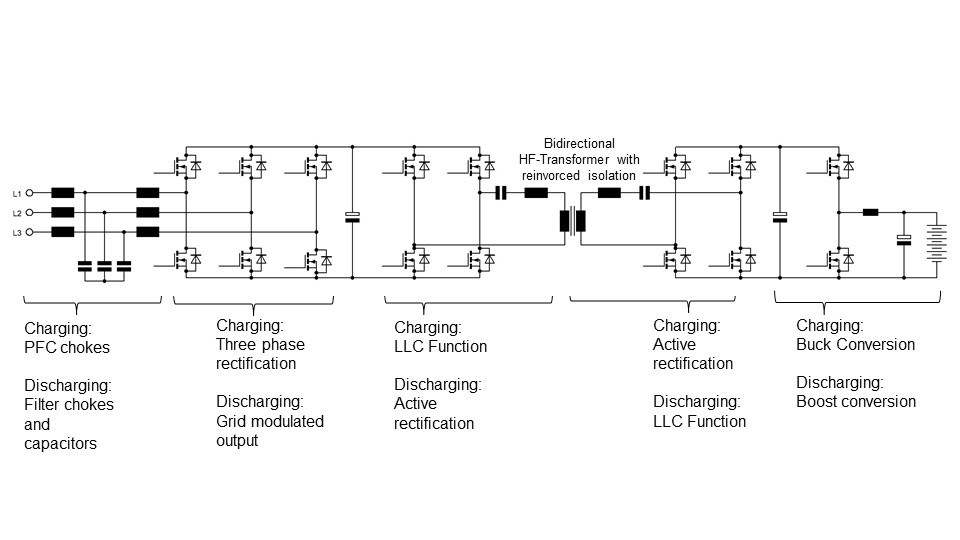
Figure 1. Bi-directional charger circuit with multiple stages of power conversion
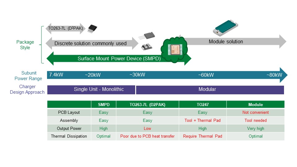
Figure 2. Packaging power capability and comparison of packaging performance
Implementation of SMPD Packaging for Higher Power Density
Designers can use SMPDs to house a wide range of chip-technologies in various voltage classes and circuit topologies, including half-bridges. Figure 3 gives an example of the packaging for an SMPD by Littelfuse. The SMPD features a Direct Copper Bonded (DCB) substrate with a copper lead frame, aluminum bond wires, and a plastic molding compound around the semiconductor. The DCB structure offers high isolation strength and allows a multi-semiconductor arrangement with high thermal dissipation capabilities on a single carrier. The exposed copper layer in the DCB maximizes the surface area for connection to a heat sink. Combining a copper lead frame with aluminum bond wires allows simplified soldering and assembly.
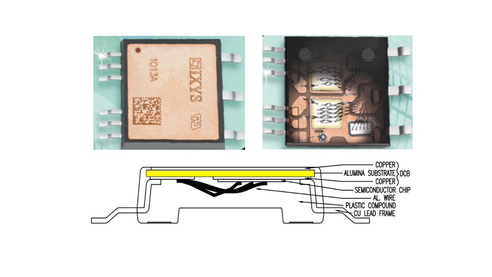
Figure 3. Example structure of a surface-mount power device (SMPD) package (source: Littelfuse)
The design of the SMPD package in this example offers several advantages:
- UL-recognized, Insulation voltage rating up to 2500 V
- Lower thermal resistance compared to other semiconductor packaging such as TO-style devices.
- SMPD provides higher current carrying capacity than available with TO-style packages.
- Reduced radiated EMI due to low parasitic coupling capacitance between the semiconductor die and the heatsink.
- Maximized utilization of the semiconductor’s capabilities and low voltage-overshoot resulting from package’s low stray inductance.
- There is greater flexibility in enabling customized topologies, including thyristors, power diodes, MOSFETs, and IGBTs.
- Because of the isolated backside, all power semiconductors can be mounted on a single heat sink.
Figure 4 highlights how SMPD packaging reduces the number of components almost by half, allowing for higher power, enhanced power density, and reduced assembly size. Each package in the example contains two power MOSFETs as one example of multiple circuit configurations available in SMPD packaging.
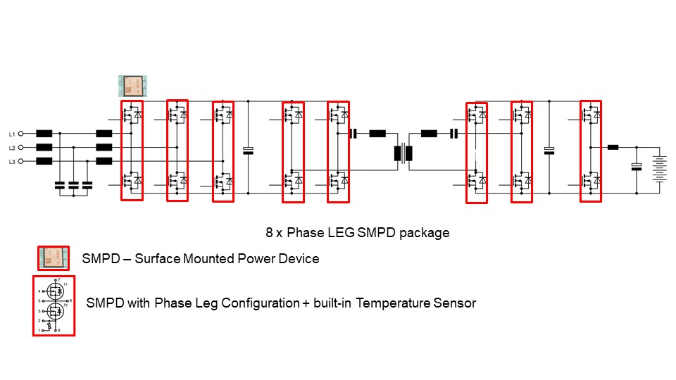
Figure 4. Bi-directional charger built on SMPD packaging to reduce the component count by half compared to using discrete devices.
Higher power in smaller packages
Designers can increase the power of their chargers and thus improve power density. By incorporating SMPD packaging, designers can develop single power units with an output as high as 50 kW without the need for paralleling components. Using SMD-style power components can lower the manufacturing cost with fewer components. Surface-mounted package designs, such as those from Littelfuse, can minimize heatsink size and cost with low thermal resistance packaging technology. With lower parasitic capacitance and stray inductance, this packaging can lower both radiated and conducted EMI. The designer can use smaller inductors by operating at higher frequencies, saving space and cost. SMPD power device packaging helps designers overcome the challenges of increasing the output power without substantially increasing size and weight of the system built.
To learn more, download the application note, Mounting and Cooling Solutions for SMPD Packages, courtesy of Littelfuse, Inc.

Sponsored by Littelfuse